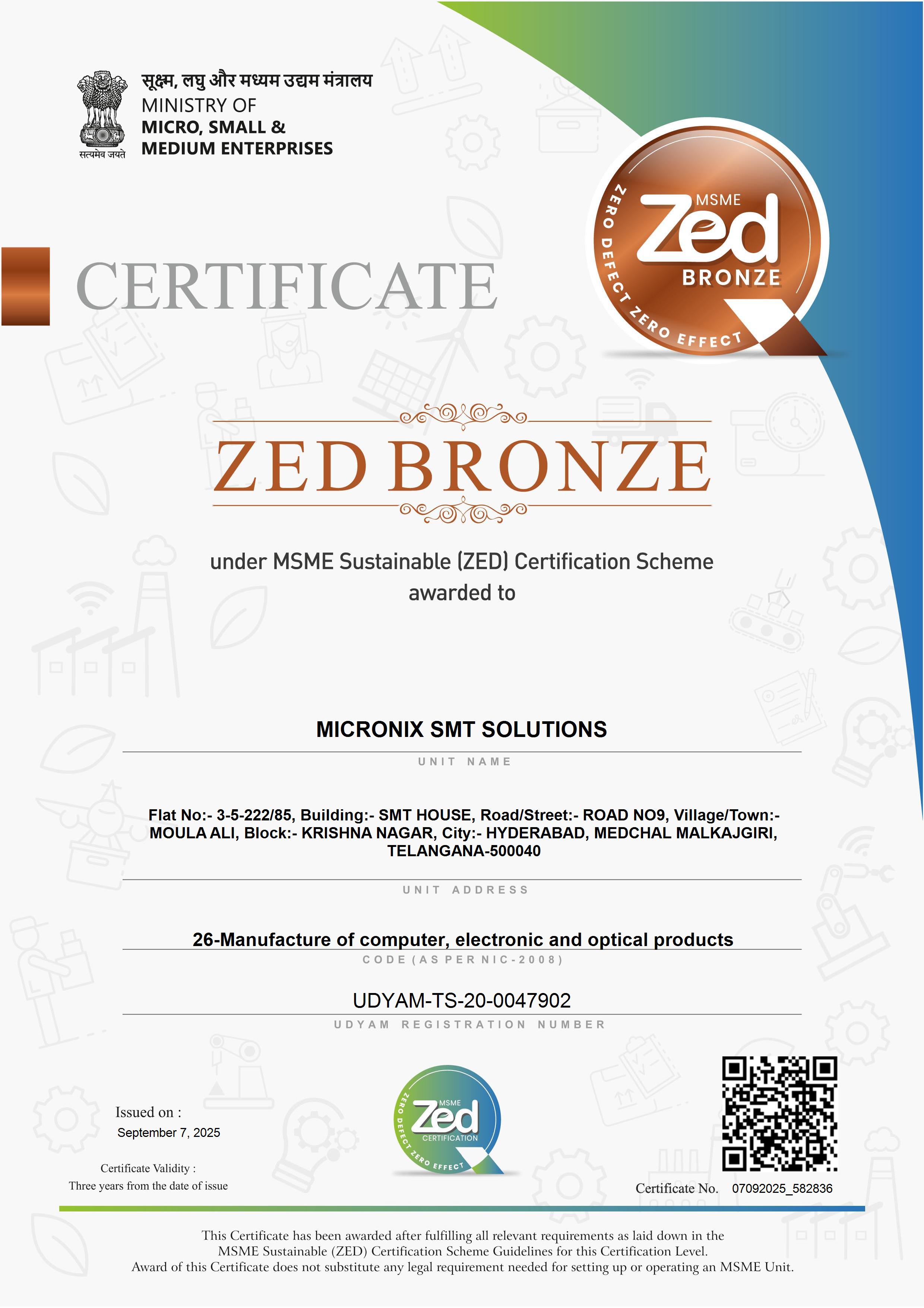
IPC-A-610 Standard
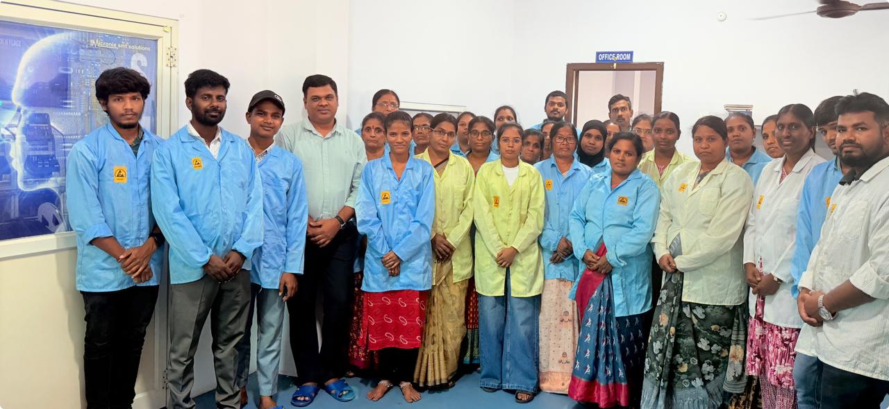
About Micronix SMT
Your Trusted Electronics Manufacturing Partner
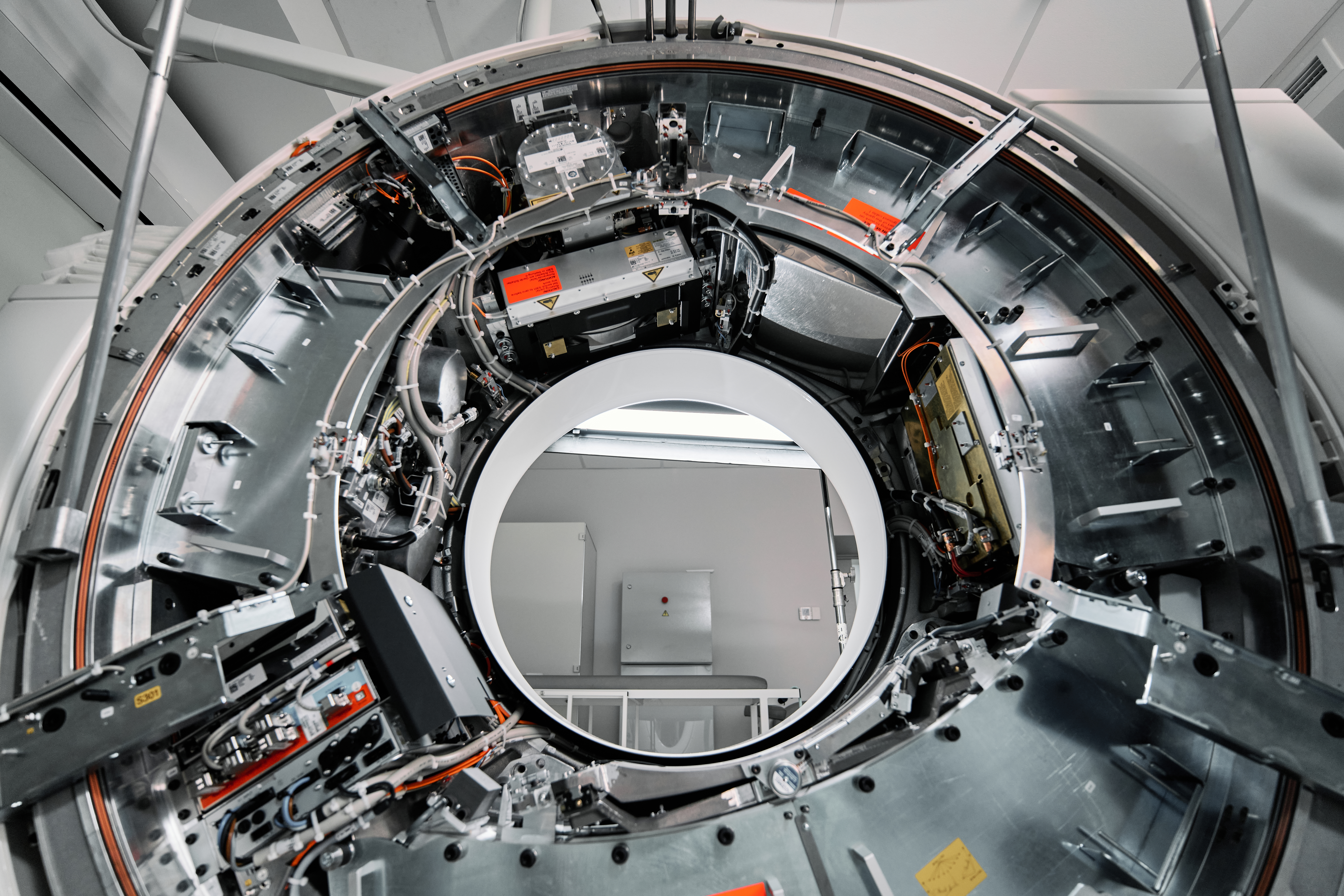
Micronix SMT Solutions is a full-spectrum Electronics Manufacturing Services (EMS) company specialising in PCBA, THT assembly, box-build, and turnkey system integration. We partner with OEMs across six critical industries to deliver precision-engineered assemblies.
-
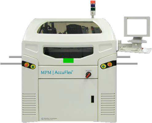
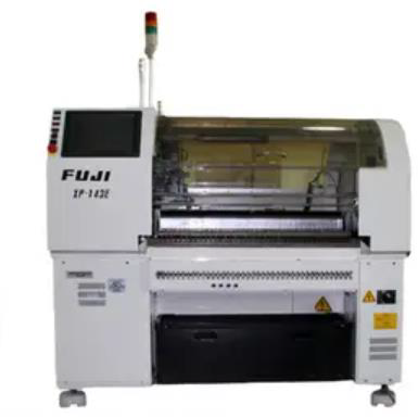
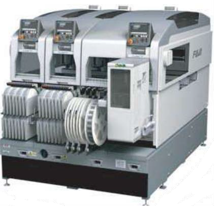
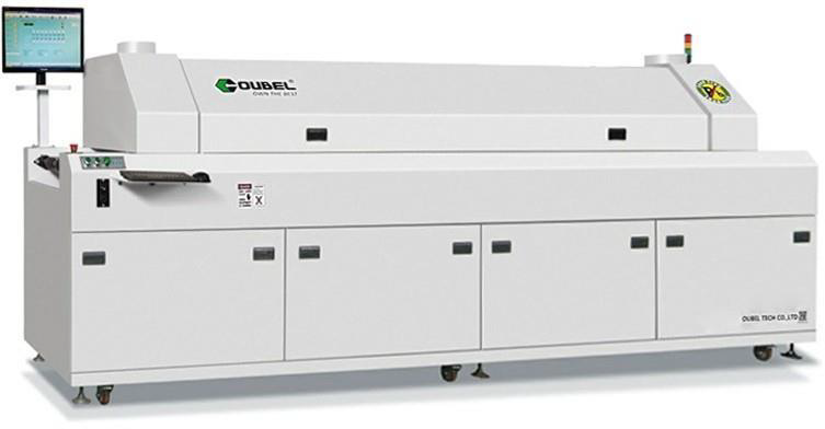
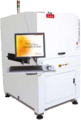
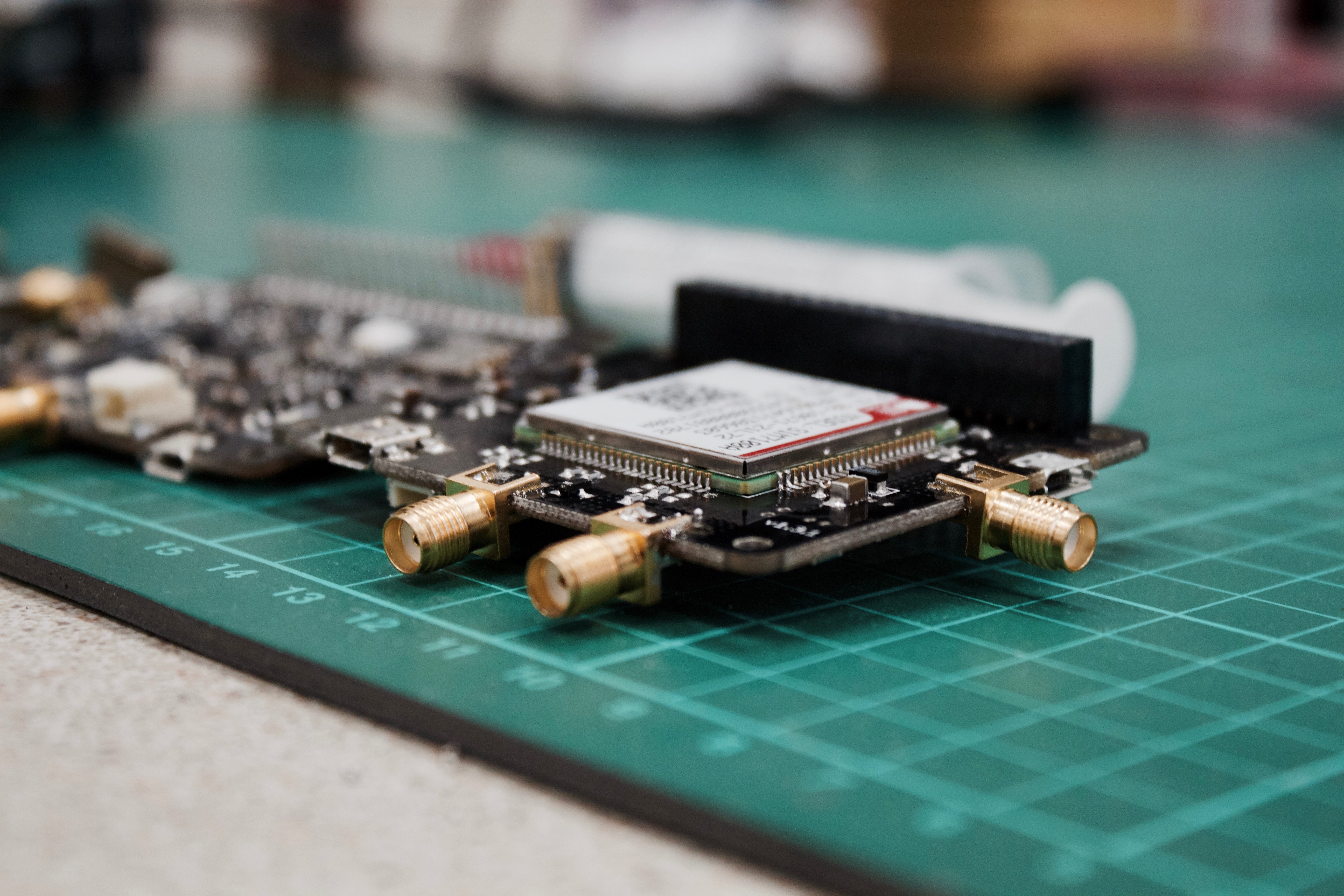
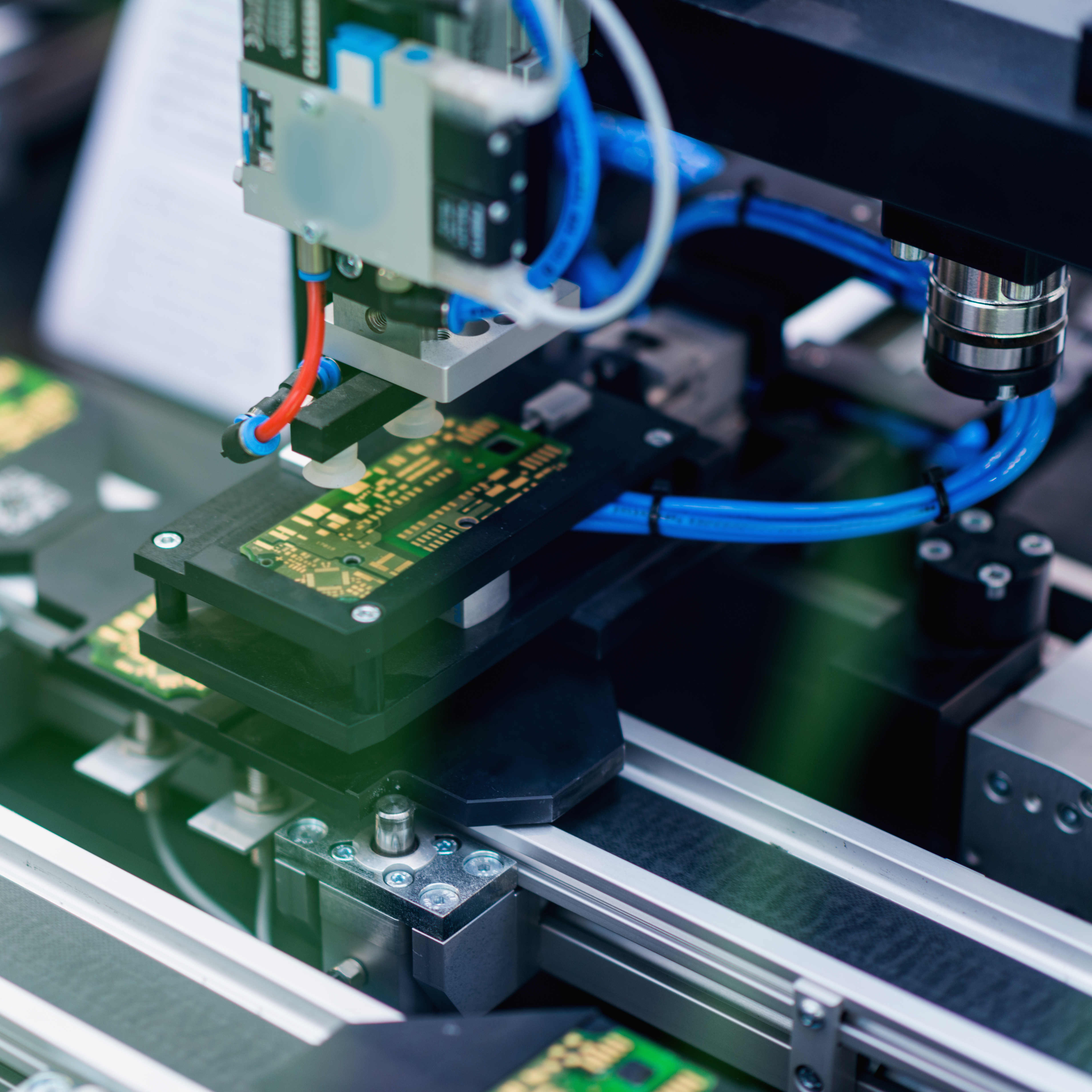
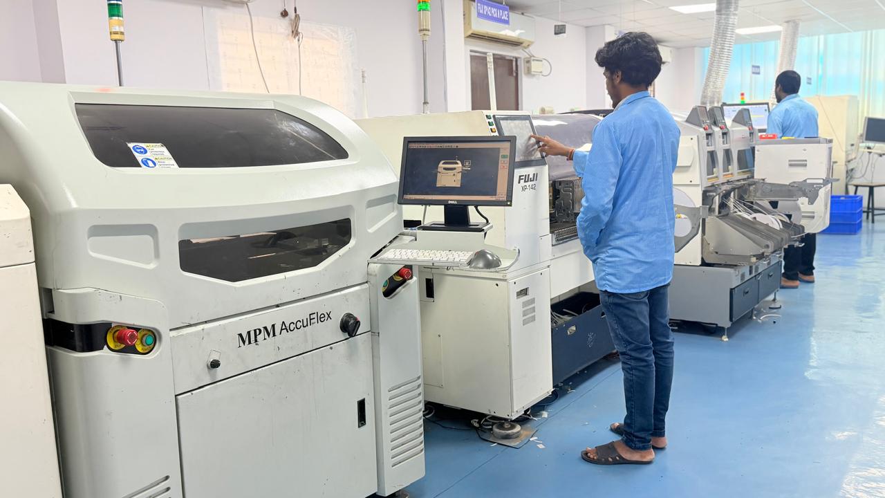
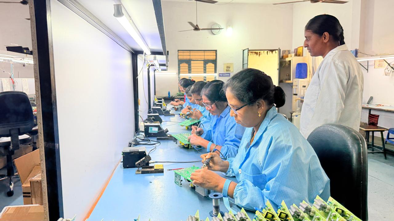
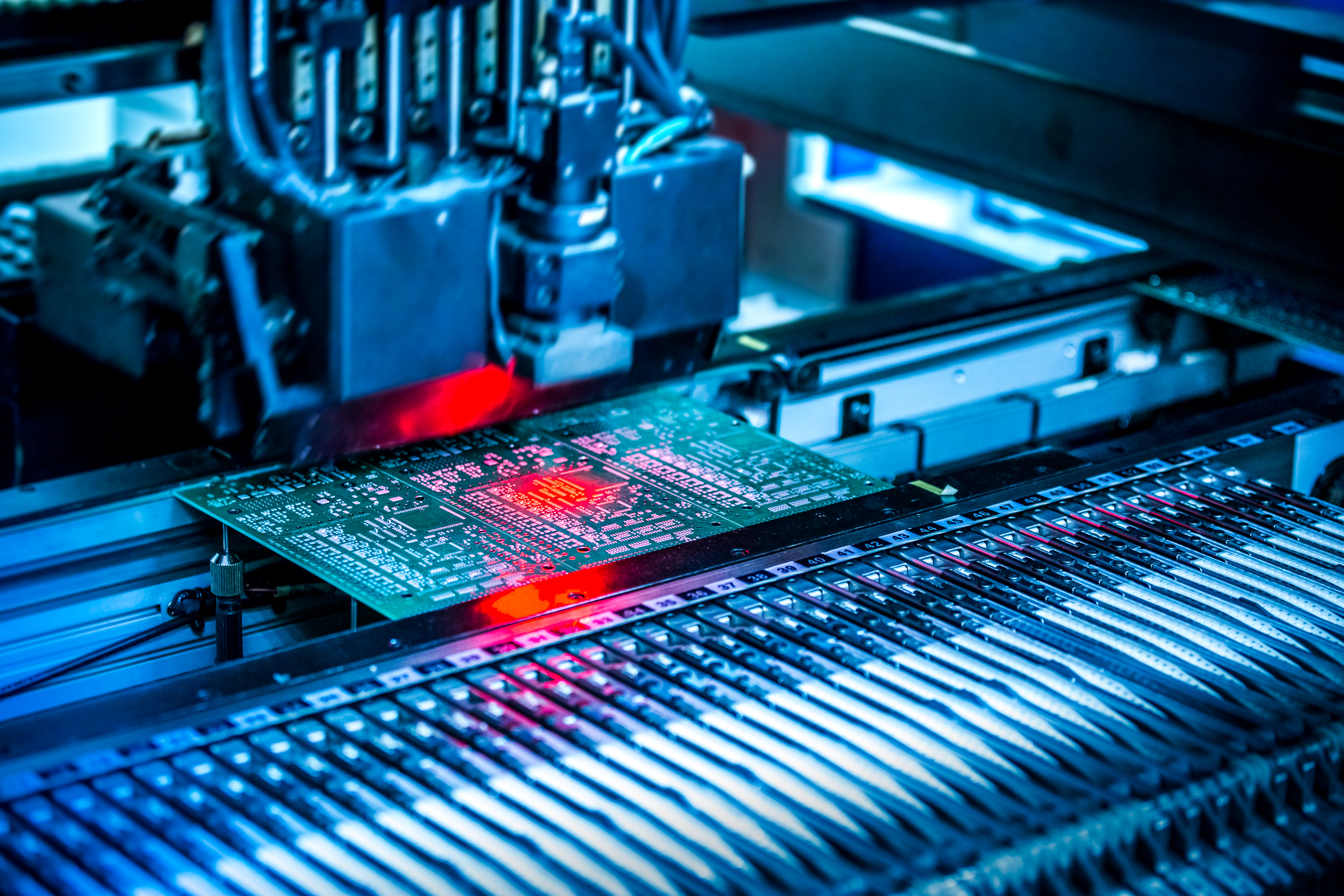
✓High-mix technology manufacturing with advanced SMT placement for complex, multi-layered boards handling fine-pitch components to 0.03mm precision
-
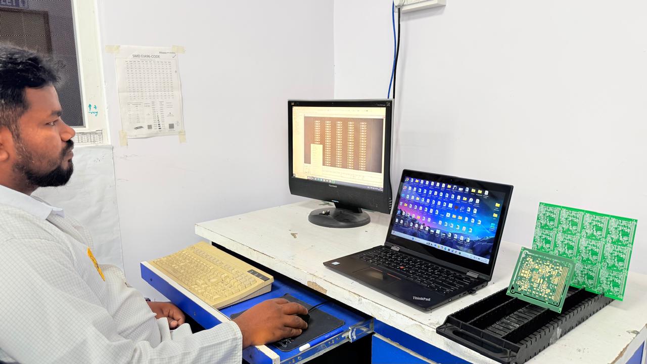
✓Fast-track NPI services — move from CAD files to functional, tested hardware without compromising quality or reliability
-
✓Full turnkey box-build assembly including mechanical housing, cable harnessing, potting, and software flashing
-
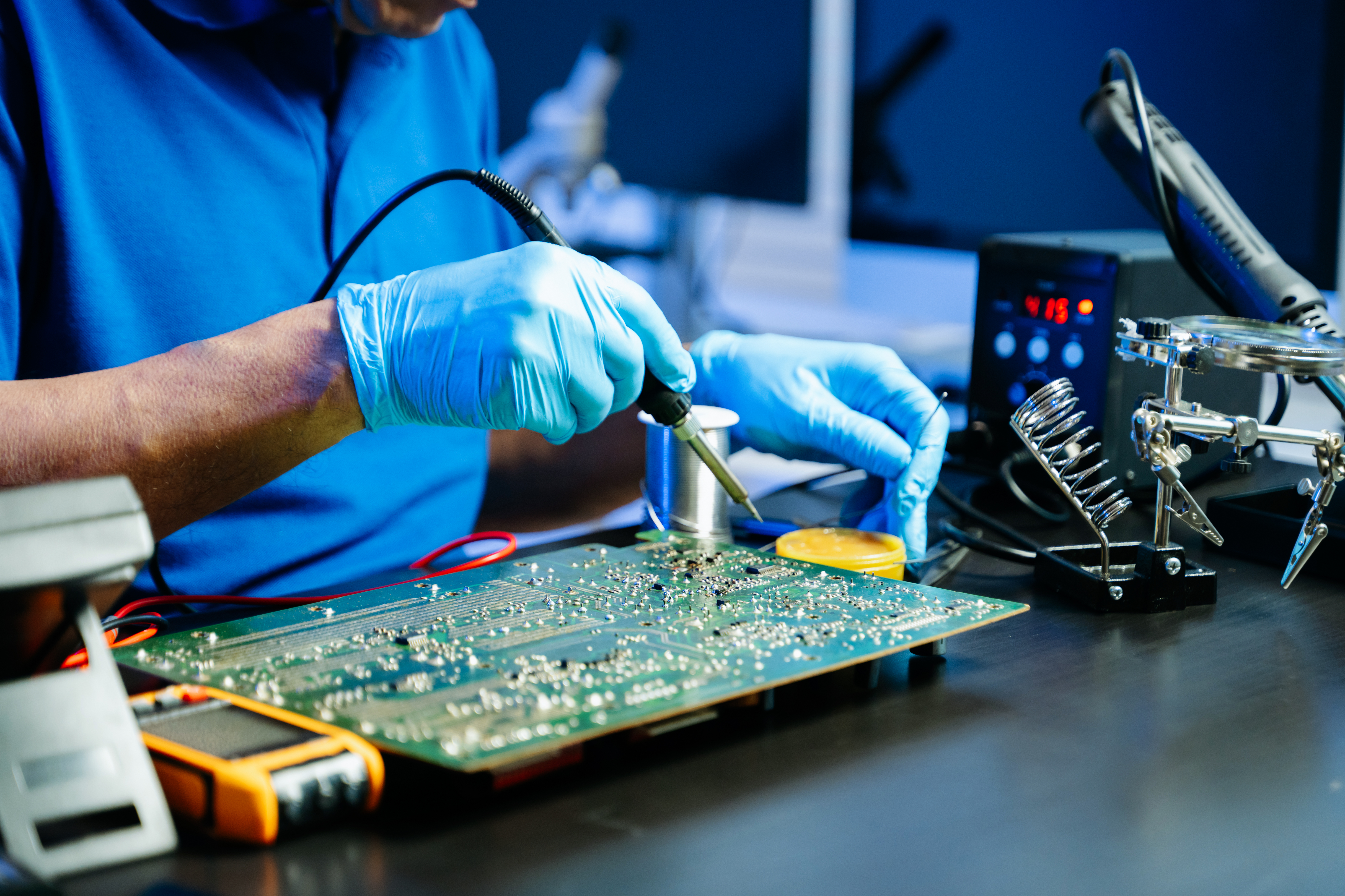
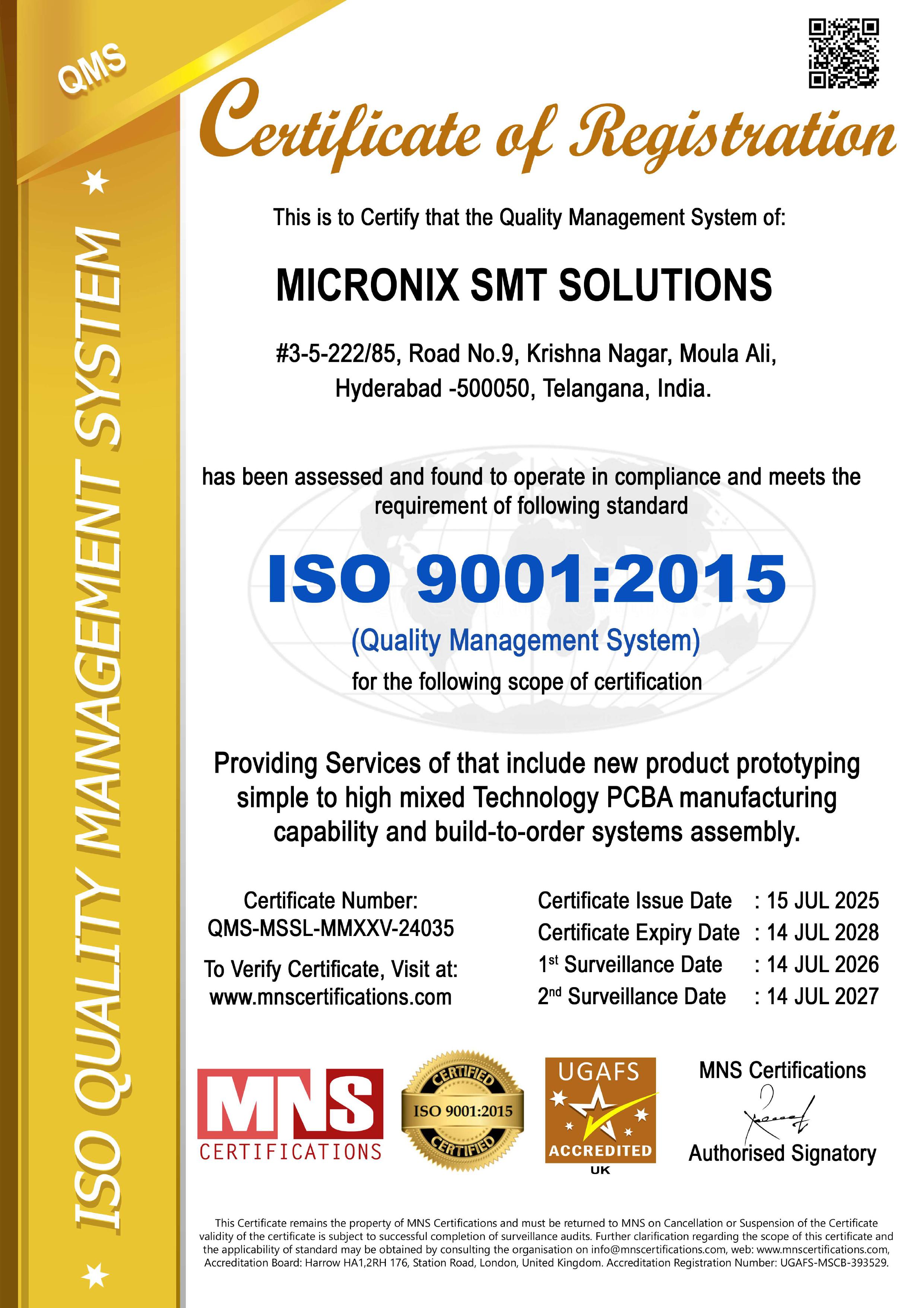
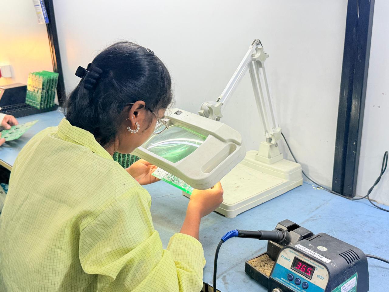
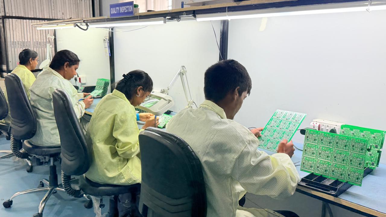
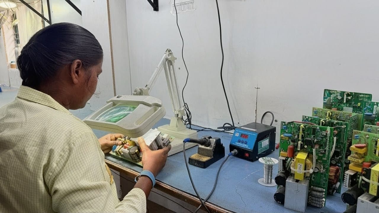
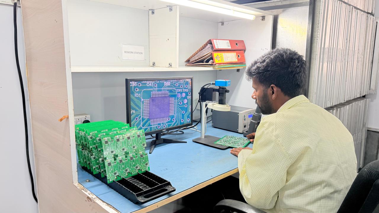
✓Rigorous AOI, ICT, and functional testing protocols compliant with IPC-A-610 international standards
-
✓Expert DFM feedback loop — catches design issues early to improve first-pass yield and reduce programme cost